
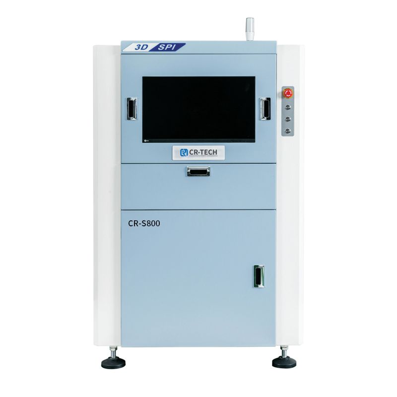
What is 3D Solder Paste Inspection
3D Solder Paste Inspection Introduction
In the highly competitive and precise world of electronics manufacturing, the quality of a solder joint is fundamental to the reliability and functionality of the final product. This quality journey begins not at the reflow oven, but much earlier, at the solder paste printing stage. Solder Paste Inspection (SPI) has thus become a critical process control step, evolving from simple 2D checks to the sophisticated, data-rich world of 3D Solder Paste Inspection. This article explores what 3D SPI is, how it works, its advantages, and its vital role in modern Surface Mount Technology (SMT) assembly lines.
From 2D to 3D: The Evolution of Inspection
Traditionally, solder paste inspection relied on 2D imaging. Cameras would capture a top-down view of the printed paste, analyzing attributes like area, position, and shape by contrasting the paste against the PCB pad. While useful for gross defects like bridging or severe misalignment, 2D inspection has a critical flaw: it cannot measure volume or height.
Solder paste volume is the single most important factor for forming a reliable solder joint. Too little paste results in a weak, "starved" joint. Too much paste can cause bridging (short circuits) or tombstoning of components. 2D inspection simply cannot detect these volumetric defects, allowing them to propagate down the line, where repair costs increase exponentially.
3D SPI overcomes this limitation by adding the crucial Z-axis dimension. It doesn't just see the paste; it measures its precise height profile, enabling the calculation of true volume for every single pad.
How Does 3D SPI Work? The Core Technologies
Modern 3D SPI systems primarily use structured light or laser triangulation techniques to capture height data.
-
Structured Light (Phase-Shift Profilometry): This is the most common method. The system projects a series of patterned, shifting light fringes (often blue or white LED light) onto the board's surface. One or more high-resolution cameras, set at a known angle, observe the distortion of these fringes as they fall over the three-dimensional solder paste deposits. Sophisticated algorithms then analyze the fringe distortions to calculate the height of every point on the board, generating a detailed 3D height map.
-
Laser Triangulation: A fine laser line or dot is scanned across the PCB. A camera positioned at an angle captures the laser's reflection. As the laser traverses over a solder paste bump, the reflected laser line's position in the camera's field of view shifts. This shift is triangulated to compute the height with very high accuracy.
The result is a rich dataset for every printed pad, including:
-
X, Y Position: Alignment with the underlying pad.
-
Height (Z): Measured at multiple points.
-
Volume: Calculated by integrating the area and height data.
-
Area & Shape: Contour and coverage analysis.
Key Measurement Parameters and Defect Detection
A 3D SPI system programmatically compares the measured 3D data against the ideal "golden" parameters from the CAD/CAM data (typically the Gerber file). It evaluates several critical characteristics:
-
Volume: The primary metric. Checks if paste is within a user-defined percentage range (e.g., ±40% of nominal).
-
Height: Measures the peak height and average height of the deposit.
-
Area: Calculates the plan-view area of the paste.
-
Bridging: Detects if paste from adjacent pads is merging, which would cause a short circuit.
-
Solder Balling/Residue: Identifies unwanted specks of solder paste outside the pad areas.
-
Shape/Flatness: Assesses the paste deposit's profile (e.g., slumped, peaked, or properly formed).
The Critical Advantages of Implementing 3D SPI
-
Dramatic Reduction in Defects: By catching volumetric defects at the source, 3D SPI prevents defective boards from proceeding to component placement and reflow, where rework is 5-10 times more expensive. It is the first and best defense against the most common solder defects.
-
Process Control and Optimization: 3D SPI is not just a "pass/fail" gatekeeper. It provides real-time, statistical process control (SPC) data. Manufacturers can monitor trends in stencil wear, printer drift, paste viscosity changes, and squeegee performance. This data allows for predictive and preventive maintenance, optimizing the printing process before it goes out of specification.
-
Enabling Advanced Packaging and Miniaturization: As components shrink to 01005, 008004 sizes, and advanced packages like µBGAs and CSPs with fine-pitch leads become common, the tolerance for printing error vanishes. 3D SPI is essential for ensuring the tiny, precise paste volumes required for these components.
-
Improved First Pass Yield and Reduced Cost: By ensuring only good prints move forward, overall line yield increases significantly. The cost savings from avoided rework, scrap, and field failures far outweighs the investment in the SPI system.
-
Closed-Loop Feedback: High-end SMT lines integrate 3D SPI in a closed-loop with the solder paste printer. The SPI measures a board, and if a systematic error (e.g., X-axis offset, insufficient volume) is detected, it automatically sends a correction signal back to the printer to adjust its parameters for the next board, creating a self-correcting manufacturing process.
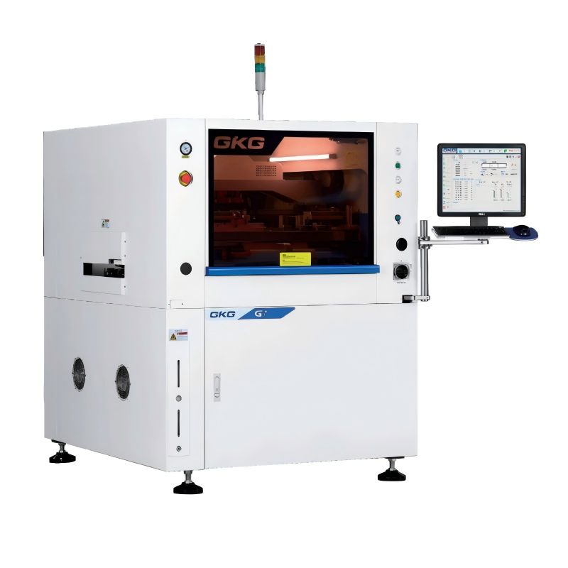
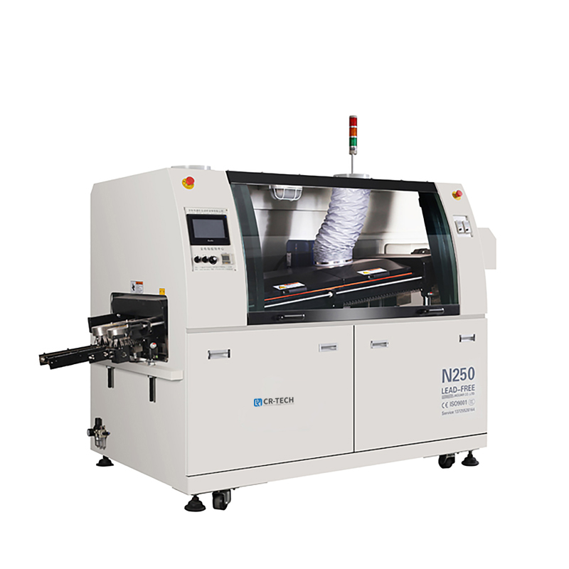
Integration into the SMT Line and Workflow
A typical 3D SPI system is placed inline, immediately after the solder paste printer and before the pick-and-place machine.
-
The PCB exits the printer and is conveyed into the SPI.
-
The board is securely fixed, and the measurement head scans the entire board in seconds.
-
Software analyzes the 3D data against pre-set acceptance criteria.
-
Results are displayed: a color-coded map (Green/Yellow/Red) shows the status of each pad.
-
The board is either passed to the next stage, sent for offline rework, or (in closed-loop systems) data is fed back to the printer.
-


