

Types of solder paste inspection
Solder Paste Inspection (SPI) Methods
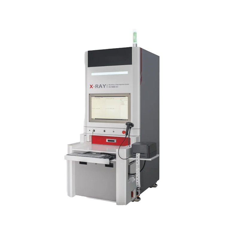
Solder paste inspection (SPI) is a critical quality control process in Surface Mount Technology (SMT) assembly, performed immediately after the stencil printing stage. As solder paste defects are the leading cause of assembly failures downstream, effective SPI is essential for preventing costly rework and ensuring final product reliability. Modern inspection methodologies have evolved from basic manual checks to highly sophisticated automated systems. This article outlines the primary SPI methods in use today.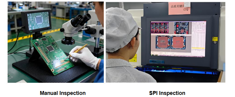
1. 3D Solder Paste Inspection (3D SPI) – The Industry Standard
This is the most advanced and widely adopted method in high-volume, high-mix electronics manufacturing.
-
Technology: 3D SPI systems use structured light, laser triangulation, or phase-shift profilometry. A common approach involves projecting a series of alternating light patterns (moire fringe patterns) onto the board. One or more cameras capture the distortion of these patterns caused by the height of the solder paste deposits. Advanced software algorithms then calculate a precise three-dimensional map of each solder paste deposit.
-
Key Measured Parameters:
-
Volume: The most critical parameter. Insufficient volume leads to weak or open joints; excessive volume can cause bridging.
-
Height: Measures the paste deposit's stature. Critical for ensuring proper standoff and post-reflow joint formation.
-
Area: Checks the X and Y spread of the paste, identifying smear, bridging, or misalignment.
-
Alignment/Offset: Measures the deposit's position relative to the solder pad.
-
Shape & Solder Ball Detection: Identifies paste scooping, poor shape, or the presence of large solder balls within the paste.
-
-
Advantages:
-
Quantitative Data: Provides accurate, measurable data for statistical process control (SPC).
-
Comprehensive Defect Detection: Capable of catching height and volume-related defects invisible to 2D systems.
-
Process Feedback: Can be integrated in-line to provide real-time feedback to the stencil printer, enabling automatic correction of misalignment or pressure.
-
-
Disadvantage: Higher initial capital investment compared to 2D systems.
2. 2D Automated Optical Inspection (2D AOI) for Solder Paste
While often associated with post-placement or post-reflow inspection, 2D AOI can be deployed after printing.
-
Technology: Utilizes high-resolution cameras with consistent, often multi-directional lighting (e.g., red, green, blue, and white) to capture a two-dimensional image of the paste deposits. The image is compared to a "golden board" reference or CAD-derived rules.
-
Key Inspected Features:
-
Presence/Absence: Detects missing deposits.
-
Bridging: Identifies solder paste connecting between two or more pads.
-
Smearing/Spread: Flags excessive paste spreading outside the pad area.
-
Gross Misalignment: Detects if the paste is significantly off-pad.
-
-
Advantages:
-
Lower Cost: Generally more affordable than 3D SPI systems.
-
High Speed: Can achieve very high throughput for simpler checks.
-
Effective for Planar Defects: Excellent for detecting bridging and smear.
-
-
Disadvantages:
-
No Height/Volume Data: Its fundamental limitation is the inability to measure paste height or volume. A deposit with perfect shape but only 50% of the required height will pass inspection.
-
Lighting Sensitivity: Performance can be highly dependent on lighting setup and board surface reflectivity (e.g., on gold or bare copper pads).
-
3. Manual Visual Inspection (MVI) with Microscope
This is the traditional and most basic method, now largely relegated to low-volume prototyping, repair stations, or as a backup spot-check.
-
Method: An operator uses a bench-mounted optical microscope or a magnifying lamp to visually examine solder paste deposits against workmanship standards.
-
Procedure: The inspector looks for obvious defects like bridging, incomplete deposits, scooping, or misalignment.
-
Advantages:
-
Very Low Cost: Requires minimal capital equipment.
-
Flexibility: An experienced operator can assess complex or unusual board areas.
-
-
Disadvantages:
-
Subjective & Inconsistent: Highly dependent on operator skill, attention, and fatigue.
-
No Quantitative Data: Provides only a pass/fail judgment without measurable process metrics.
-
Slow and Non-Exhaustive: Impractical for modern, dense boards with thousands of deposits. It is a sampling technique, not 100% inspection.
-
No Height Assessment: Like 2D AOI, cannot gauge volume.
-
The Process Control Loop: Integrated SPI
The greatest value of automated SPI, particularly 3D SPI, is realized when it is integrated into the SMT line. In a closed-loop system, the inspection machine communicates directly with the stencil printer. If a repeating defect pattern is detected (e.g., deposits on one side of the board are consistently low), the SPI system sends a correction command to the printer to adjust its pressure, alignment, or cleaning cycle. This real-time feedback stabilizes the printing process, reduces defects, and minimizes waste.
Conclusion
The choice of solder paste inspection method depends on product complexity, volume, and quality requirements. For most modern manufacturing, 3D SPI is the de facto standard, providing the essential volumetric data needed for robust process control and zero-defect goals. 2D AOI serves as a more budget-conscious option for catching gross planar defects where height is less critical. Manual inspection, while largely obsolete for production, remains a useful tool in lab and repair environments. Ultimately, implementing an appropriate and automated SPI strategy is not merely an inspection step but a fundamental pillar of process optimization in SMT assembly, directly impacting yield, cost, and product reliability.


