
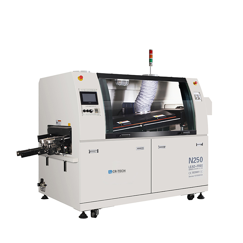
Wave soldering and reflow soldering
Reflow Soldering vs. Wave Soldering: A Comprehensive Comparison in Electronics Manufacturing
In the intricate world of electronics manufacturing, the creation of reliable and functional printed circuit board assemblies (PCBAs) hinges on the precise and permanent attachment of components. Two dominant soldering techniques form the backbone of this process: Reflow Soldering and Wave Soldering. While both aim to form robust electrical and mechanical connections, their principles, processes, and applications are distinctly different. This article provides a detailed comparison, explaining their mechanisms, step-by-step workflows, inherent advantages and limitations, and ideal use cases.
1. Fundamental Principles and Core Concepts
Reflow Soldering is a selective, surface-level soldering process primarily used for attaching Surface Mount Devices (SMDs). Its core principle involves applying a solder paste—a homogeneous mixture of microscopic solder spheres and flux—onto the PCB's solder pads. Components are then precisely placed on this paste. The entire assembly passes through a precisely controlled, multi-zone oven called a reflow oven. Here, the temperature is raised according to a specific profile, causing the solder paste to melt (reflow), wet the component leads and PCB pads, and then cool down to form permanent solder joints.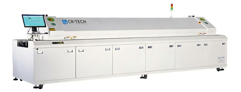
Wave Soldering, in contrast, is a bulk, through-hole oriented process. It is designed to solder the leads of Through-Hole Components (THCs) that are inserted into pre-drilled holes on the PCB. The defining element is a pumped, molten wave of solder. The PCB, with components inserted on its top side, is conveyed over this wave. The crest of the solder wave contacts the underside of the board, simultaneously filling the plated through-holes and soldering all exposed metallic surfaces (component leads and PCB pads/holes) in one pass.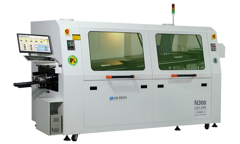
2. Detailed Process Breakdown
A. Reflow Soldering Process (典型 4-step process):
-
Solder Paste Application: Solder paste is precisely deposited onto the PCB pads using a stencil printer and a laser-cut stainless steel stencil.
-
Component Placement: A high-speed, automated pick-and-place machine accurately positions SMDs onto the pasted pads.
-
Reflow Heating: The populated PCB travels through the reflow oven's zones:
-
Preheat: Gradually raises temperature to activate flux and evaporate solvents.
-
Thermal Soak: Stabilizes temperature, ensuring even heating across the board.
-
Reflow (Peak): Temperature exceeds the solder's melting point (typically 217-250°C for SAC alloys), causing it to melt, flow, and form intermetallic bonds.
-
Cooling: Controlled solidification to form reliable, shiny joints.
-
-
Inspection & Cleaning: Automated Optical Inspection (AOI) and, if needed, cleaning to remove flux residues.
B. Wave Soldering Process (典型 6-step process):
-
Flux Application: The bottom side of the PCB is coated with flux (via foam, wave, or spray) to clean surfaces and prevent oxidation.
-
Preheating: The board is preheated to avoid thermal shock, activate the flux, and begin evaporating solvents.
-
Wave Contact: The preheated PCB is conveyed over the molten solder wave. A "turbulent" wave often penetrates holes, followed by a "laminar" wave to finish the joint and remove excess solder (icicles).
-
Cooling & Solidification: The board exits the wave, and joints cool and solidify, usually with forced air.
-
Cleaning: Critical for rosin-based fluxes, less so for no-clean formulations. Removes corrosive residues.
-
Inspection & Touch-Up: Manual or automated inspection for defects like bridges, voids, or insufficient fill, often requiring manual repair.
3. Comparative Analysis: Advantages and Disadvantages
| Feature | Reflow Soldering | Wave Soldering |
|---|---|---|
| Component Type | Optimized for Surface Mount Devices (SMDs). | Optimized for Through-Hole Components (THCs). Can solder some SMDs on bottom side (with adhesive). |
| Process Complexity | High initial setup (stencil, profile). Highly automated and repeatable once running. | Mechanically complex (wave dynamics, maintenance). Process parameters (angle, speed) require fine-tuning. |
| Joint Quality & Reliability | Excellent for SMDs. Consistent, controlled joints. Less thermal stress on board. | Excellent for THTs, providing strong mechanical bonds. Higher thermal stress on PCB and components. |
| Solder Material Efficiency | Very efficient (paste only where needed). Minimal waste. | Less efficient. Significant solder dross (oxidized waste) generation, requiring constant management. |
| Design Flexibility & Density | Enables miniaturization and high-density layouts (fine-pitch, BGAs). Double-sided assembly easy. | Limited by hole spacing. Bottom-side layout is restricted due to wave contact. |
| Primary Defects | Solder bridging (fine-pitch), tombstoning, voids, cold joints, head-in-pillow (BGAs). | Solder bridges (between pins), icicles, insufficient hole fill, shadowing (from components), flux residues. |
| Operational Cost & Energy | Lower ongoing consumable cost (paste). Energy-intensive for the oven. | High consumable cost (solder bar, flux). High energy to maintain solder pot molten (24/7 often). |
| Environmental Impact | Generally lower waste. Potential for VOC emissions from paste. | Higher waste (dross). Flux fumes require robust filtration systems. |
4. Application Scenarios and Industry Trend
Reflow Soldering is the dominant, default process in modern electronics, used for the vast majority of consumer, computing, telecommunications, and automotive electronics where SMDs prevail. It is essential for any board with fine-pitch components, Ball Grid Arrays (BGAs), or Quad Flat No-leads (QFN) packages.
Wave Soldering remains crucial for specific applications:
-
High-Power/High-Stress Electronics: Where through-hole connectors, large transformers, or capacitors require superior mechanical strength.
-
Electromechanical Assemblies: Boards with connectors, relays, or switches subject to frequent plugging/unplugging or vibration.
-
Cost-Sensitive, Legacy, or Ruggedized Devices: Simple designs or those requiring the robustness of through-hole technology.
The Hybrid Approach: Many complex PCBAs use both processes. A board undergoes reflow soldering first to attach all top-side (and sometimes bottom-side) SMDs. Then, through-hole components are manually or automatically inserted, and the board is processed through a wave soldering machine to solder these THTs and any bottom-side SMDs that were glued in place. This leverages the strengths of both technologies.
Conclusion: A Complementary Duo
In summary, reflow soldering and wave soldering are not competitors but complementary technologies serving different needs within the electronics assembly ecosystem. The choice is fundamentally dictated by component technology:
-
Choose Reflow Soldering for modern, miniaturized, high-density SMD-based assemblies. It offers precision, efficiency, and is the engine of today's electronics miniaturization.
-
Choose Wave Soldering for assemblies requiring the mechanical robustness of Through-Hole Technology or for mixed-technology boards in a hybrid process.
Understanding their distinct principles, processes, and trade-offs is essential for PCB designers, process engineers, and manufacturers to select the optimal, most reliable, and cost-effective soldering strategy for any given product. The trend towards miniaturization favors reflow, but the enduring need for mechanical reliability ensures wave soldering's continued role in the manufacturing landscape.


