
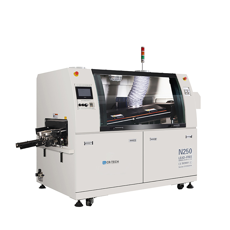
SMT Wave Soldering Working Principle and Process Flow
SMT Wave Soldering: Working Principle and Process Flow
Note: "SMT Wave Soldering" is technically a misnomer. Wave soldering is primarily a Through-Hole Technology (THT) process. However, it is used for certain Surface Mount Technology (SMT) components in a mixed-technology (SMT & THT) assembly or for specific, robust SMDs (like resistors, capacitors, LEDs) on the bottom side of the PCB. For pure SMT assembly, reflow soldering is the standard process.
This explanation covers the principle and process when SMT components are involved.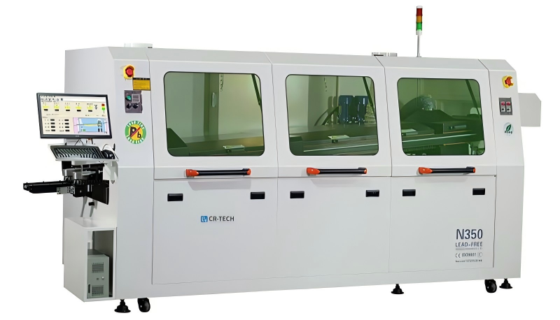
I. Working Principle
The core principle is to create a steady, flowing wave of molten solder (a mixture of tin and lead or lead-free alloys). The printed circuit board (PCB), with components pre-placed on its bottom side, is conveyed over this wave. The solder makes contact with the exposed metal pads and component leads, wicking up to form reliable solder joints through capillary action and metallurgical bonding.
Key Physical/Chemical Principles:
-
Capillary Action: Solder is drawn into the small gap between the component lead/pad and the PCB hole/pad.
-
Wettability: The flux cleans the metal surfaces, allowing the molten solder to adhere (wet) to them.
-
Surface Tension: Helps shape the solder fillet and pull excess solder off the board as it exits the wave.
-
Heat Transfer: The molten solder (~250-265°C) rapidly heats the components and PCB to form the intermetallic bond.
II. Process Flow (Step-by-Step)
The process is linear and continuous on a conveyorized wave soldering machine.
Step 1: Flux Application
-
Purpose: To remove oxides from metal surfaces, prevent re-oxidation during heating, and improve solder wettability.
-
Methods:
-
Foam Fluxing: A porous stone creates a foam wave through which the PCB passes.
-
Wave Fluxing: A wave of liquid flux is applied.
-
Spray Fluxing (Most Common): A fine, controlled mist of flux is sprayed. This is preferred for SMT as it allows better control and avoids excess flux in small gaps.
-
Step 2: Preheating
-
Purpose:
-
Activate the Flux: Drive off volatile solvents, initiating the chemical cleaning action.
-
Thermal Shock Prevention: Gradually raise the temperature of the PCB and components to minimize stress when entering the solder wave.
-
Moisture Evaporation: Prevent solder splattering.
-
-
Typical Preheat Temperature: 80-120°C on the PCB top side. Critical for preventing tombstoning of small SMT components.
Step 3: Wave Soldering
The PCB travels over the molten solder pot. Modern systems often use a double-wave structure for assemblies containing SMT components.
-
a) First Wave - Turbulent Wave:
-
A high-pressure, turbulent wave of solder.
-
Its chaotic flow ensures penetration into every area, breaking surface tension barriers and reaching all pads and leads. It is essential for soldering SMT components as it provides the mechanical force to contact the underside of the chip.
-
-
b) Second Wave - Laminar (Smooth) Wave:
-
A calm, smooth, flowing wave.
-
Its purpose is to remove bridges (shorts) created by the turbulent wave and to form clean, reliable solder fillets. It "wipes" the bottom of the board as it exits.
-
Step 4: Cooling
-
After exiting the wave, the PCB moves through a cooling zone (often forced air).
-
Purpose: Solidify the solder joints quickly to ensure a strong, reliable crystalline structure and allow immediate handling.
III. Key Considerations for SMT Components in Wave Soldering
-
Adhesion: SMT components must be glued (epoxy adhesive dot) to the PCB before soldering to prevent them from falling off into the solder pot.
-
Component Orientation: For two-pin components (like resistors, capacitors), they should be oriented perpendicular to the solder flow direction to minimize bridging.
-
Shadowing: Larger SMT components can "shadow" smaller ones downstream, preventing solder contact. Careful layout and wave dynamics are crucial.
-
Thermal Mass: Large SMT components may need higher preheat to ensure adequate joint formation.
-
Solder Mask & Pad Design: High-quality solder mask between pads and well-designed pad geometries (NSMD vs. SMD) are critical to prevent bridging and ensure good fillets.
IV. Advantages & Disadvantages for SMT
-
Advantages:
-
Can solder both THT and bottom-side SMT in a single pass.
-
Cost-effective for high-volume, simple boards.
-
Excellent for connectors and other high-reliability through-hole parts.
-
-
Disadvantages vs. Reflow for SMT:
-
Higher thermal stress on components.
-
Higher defect rates (bridging, icicles) for fine-pitch SMT.
-
Requires adhesive for SMT parts.
-
Not suitable for double-sided all-SMT boards.
-
Higher solder consumption.
-
V. Typical Defects
-
Bridging/Shorts: Solder connects two adjacent leads.
-
Tombstoning: A small SMT component stands up on one end.
-
Solder Balls: Small spheres of solder splattered on the board.
-
Insufficient/Excessive Solder.
-
Voiding: Gas bubbles trapped in the joint.
Conclusion
While reflow oven soldering dominates pure SMT assembly, wave soldering remains a vital process for mixed-technology PCBs or specific high-volume, cost-sensitive applications with robust SMT components on the bottom side. Its success hinges on meticulous process control—flux chemistry, thermal profiling, wave dynamics, and PCB design.


